Application of complementary transmission electron microscopy techniques for characterizing of advanced materials
IntroductionThe progress in designing new transmission electron microscopes achieved in recent years resulted in significant improvement not only of their resolution but also of functionality. The former - allowing to pushed it below 1Angstrom - was realized first by wide introduction of Field Emission Guns (FEG) and second by astigmatism correcting system (Cs correctors). The latter, equally important, made possible to construct microscopes with tightly spaced objective pole pieces still accepting Energy Dispersion System (EDS) detectors, which in a way helped to get both High Resolution Electron Microscope (HREM) and Analytical Electron Microscope (AEM) in one machine, like TECNAI G2 FEG (200kV).
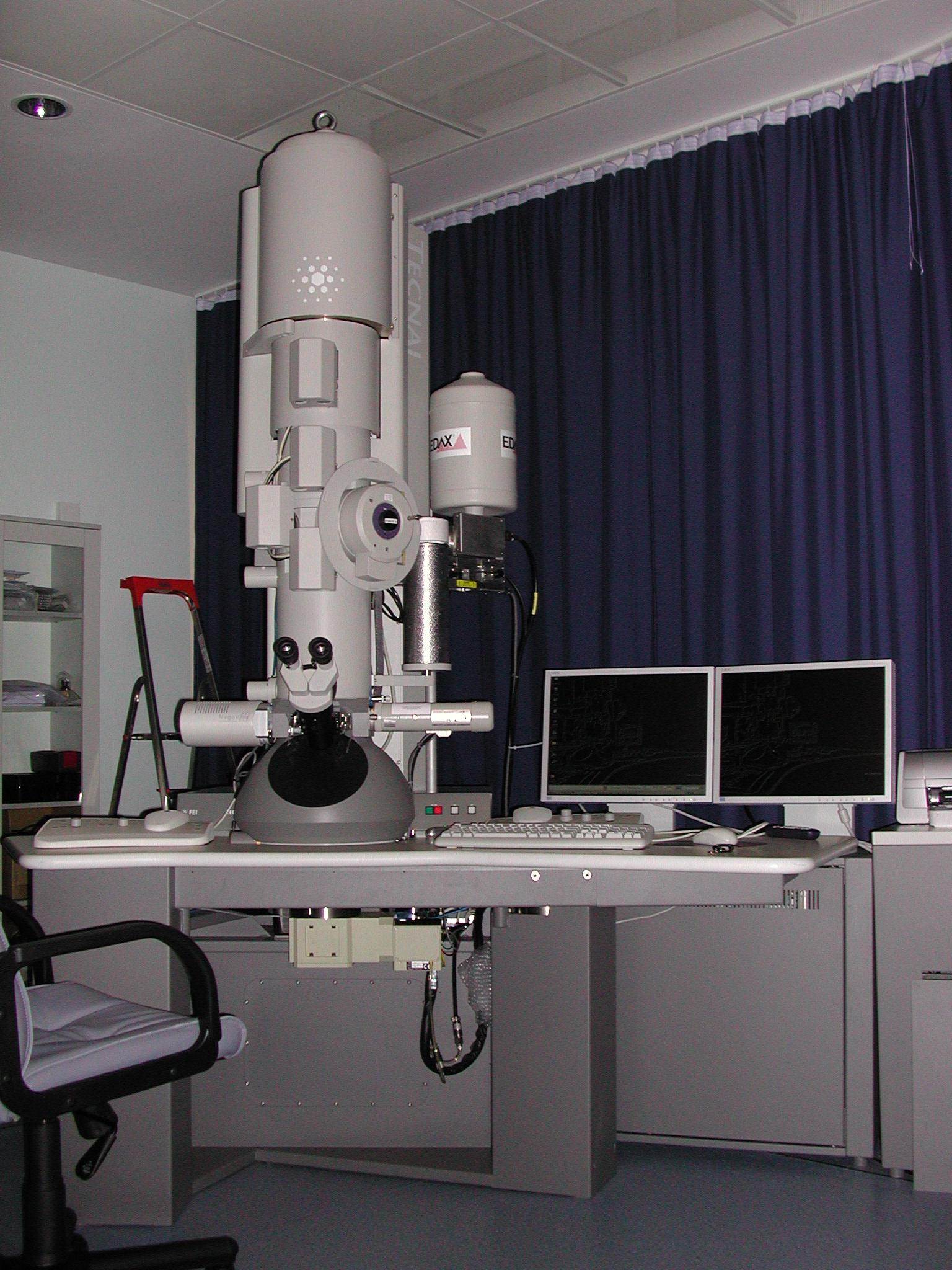
Having two microscopes in one is very convenient but performing lattice imaging and microanalysis from the very same place is rarely realized as optimum condition for each technique requires different foil thickness. The few nanometers best for high quality HREM are usually not enough for excitation of enough X-rays guaranteeing reasonably statistics for EDS spectra. Additionally, the low indices zone axis orientation necessary for the former may infer serious overrepresentation of some elements due to channeling effect making any quantitative estimates totally wrong. The determining of local orientation with convergent beam electron diffraction (CBED) calls for even thicker foils and at the same time better, more crisp lines are obtain with microscopes equipped with standard for the last twenty years LaB6 cathode. The problem with simultaneous application of chosen transmission microscopy techniques to the same feature in the microstructure is not general but it exists and should be taken into account during observations.
Performing microstructure observation and gathering other information on local phase content, orientation, stresses or chemical composition is possible with high spatial resolution only as long at a specimen of necessary for such task quality, i.e. extremely thin, clean and undisturbed by sample preparation procedure. Nowadays, after more than half of century of vigorous and wide use of transmission electron microscopy in laboratories world wide the sample preparation equipment is both precise and versatile. Aside from electro-polishing, the argon ion milling and gallium ion cutting (Focus Ion Beam - FIB) are at hand. The last two are more versatile allowing to work not only with metals but also with semiconducting and ceramic materials. The FIB offers unique opportunity to pick up place from which a sample is cut out using scanning microscope. However, these techniques tend also to heat up thinned pieces, implant particles from the operating beams and amorphise more beam sensitive materials.
The advanced materials, which get their name due to significantly improved properties or functions over those proper for their predecessor, were elaborated to large extent either by scaling down of their microstructure to nano-meters or executing full control over the material interfaces. Theoretically, the transmission electron microscopy can easily guarantee full control over material features, even at such a small scale. The described above problems with both gathering information from the same place with different techniques and preparation of acceptable for such investigation samples shows that the practical execution of it, is far from easy. The success margin for obtaining so much required information in so complicated case is therefore small, but may be significantly widened by careful planning of the experiment.
Examples
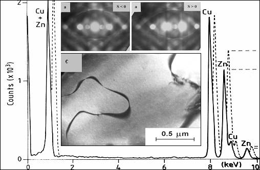
Planning may mean turning the table in a way that the disadvantages would help to get the hard to get otherwise information, like with using called Atom Location with Channeling Enhanced Microanalysis (ALCHEMI). The acquiring two EDS of spectra at orientation close to two beam condition - which are normally avoided -can help to pin-point distribution of alloying addition on planes filled with different atoms. The discussed situation representing so called "planar ALCHEMI" is best exemplified in case of fully B2 ordered brass (confirmed by presence of antiphase domain boundaries - Fig. 2c), of which copper and zinc atoms alternatively occupy {100} planes. Tilting thin foil close to two beam condition (000, 200) in a way, so its orientation is changed from s<0 to s>0 (Fig. 2 a,b) shifts the maximum of electron current of the beam from one set of planes to the other influencing the number of excited x-rays from respective elements. Setting the EDS system in a way it stops acquiring for the same value of Cu_K???the Zn_K? is much higher for the second orientation (Fig. 2). Quantification of such spectra, obtained from the same place, would give Zn content at 39 or 45 at. % respectively, what is far outside acceptable error of ą2 at% at worst. Therefore, such experiment serves solely to estimate the channeling conditions in that type of materials.
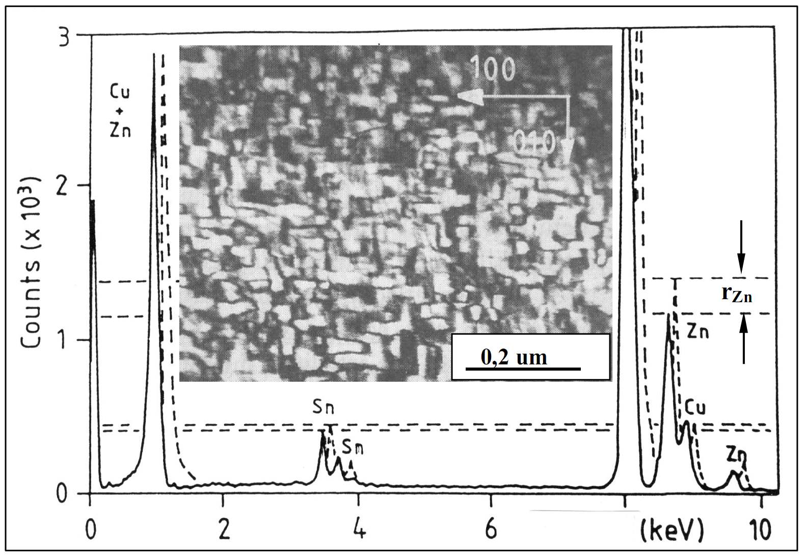
The tin addition to brass should result in its preferential occupation of zinc rich {100} planes, but both extent and kinetic of this process is of interest due to its influence on shape memory effect. Using the same approach as before, one can tilt the foil to (000, 200) two beam condition and acquire spectra at s<0and S>0 setting the Cu_K? to certain value (Fig.3). Next, it is just enough to determine weather the Sn_L? follows the changes or acts in opposite way of Zn_K? peak, what would mean that it locates on Zn or Cu rich planes respectively. The lack of response to tilting close to (000, 200) orientation would mean that addition is distributed in equally probably way on both type of planes.
The ALCHEMI show its strength best with multi-element oxide as originally elaborated by J. Spence, but was found less successful with intermetallic like NiAl. The brasses or bronzes were even more problematic as their reference ordered lattice is not fully segregated but just enriched in Cu and Zn(Al) respectively. What is more, the introduced additions should be big enough to give measurable changes during tilting close to two beam orientation. Simultaneously, increasing "probe", i.e. introduced addition causes disordering of the reference lattice. The above problems preclude quantitative assessment of ordering of introduced alloying additions, but qualitative assessment is in such case also important.
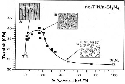
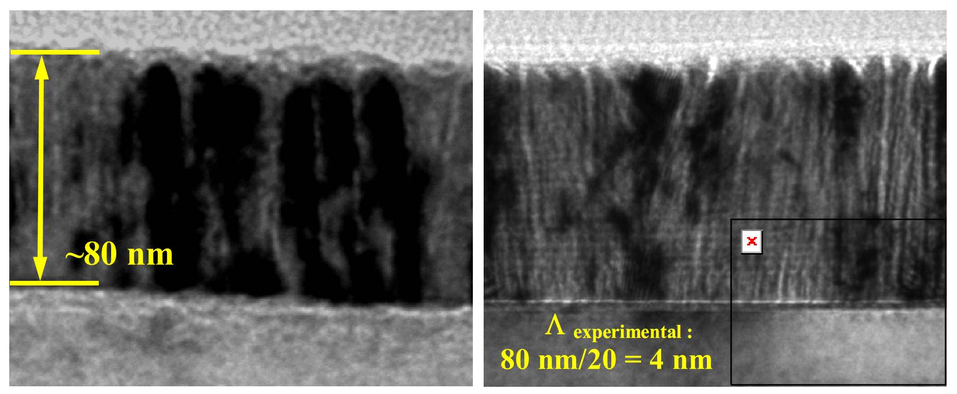
The geometrical aspects are also crucial in analysis of nano-composite amorphous - crystalline c-CrN/a-Si3N4 coatings. Their excellent properties including super-hardness can easily explained on the basis of formation of nano-composite material (Fig. 4). However, the superposition of columnar grains in such coatings made it practically impossible to confirm presence of thin sheets of amorphous material in-between them (please compare Fig. 4, image B and Fig.5).
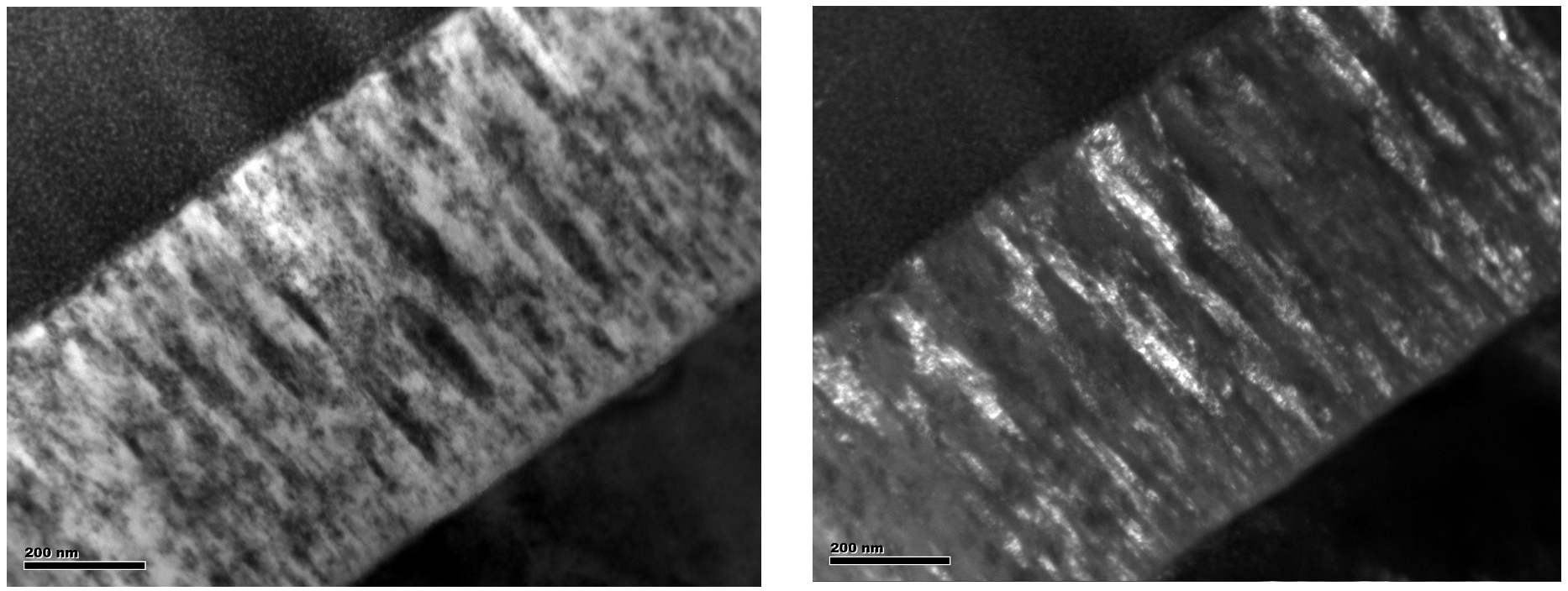
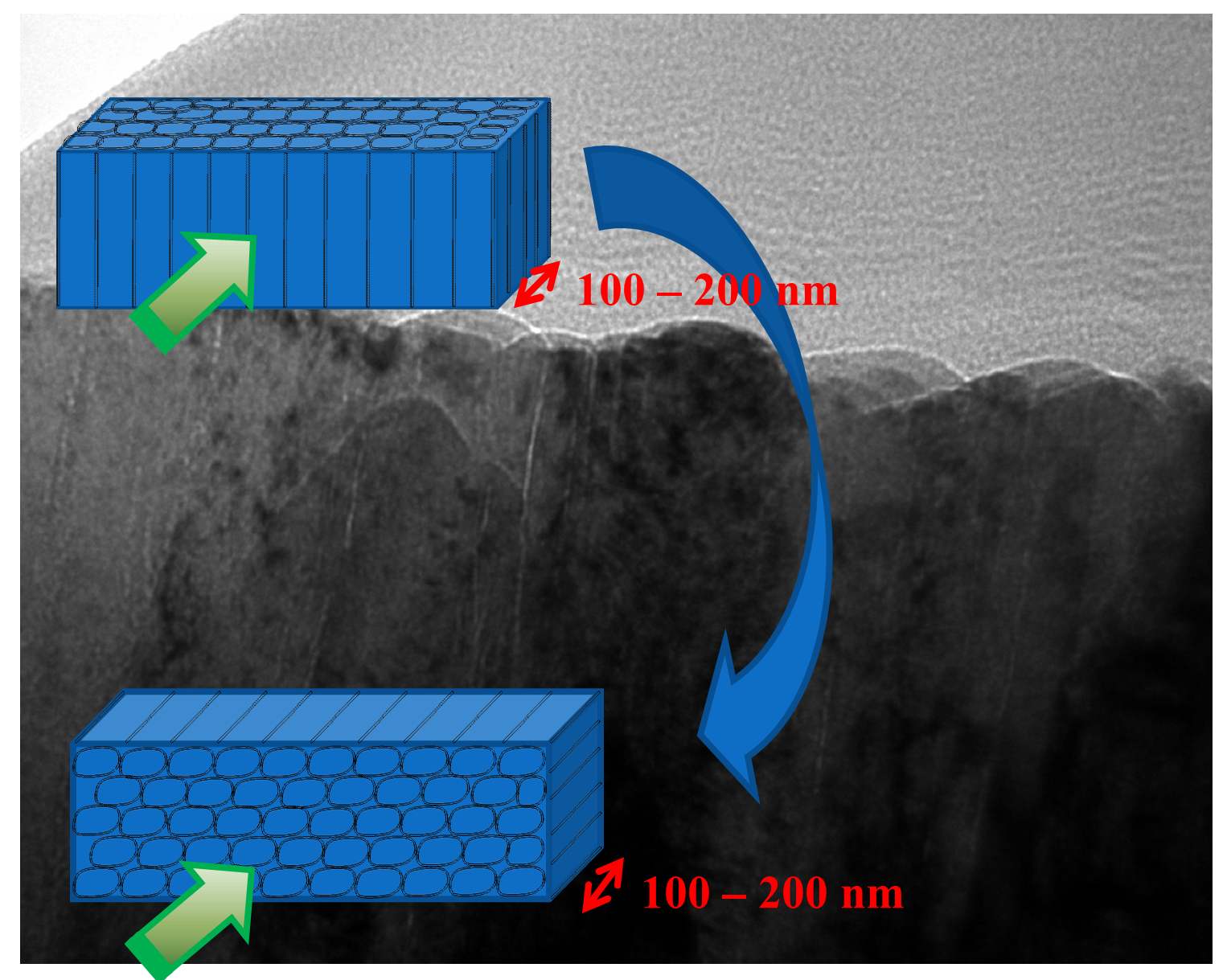
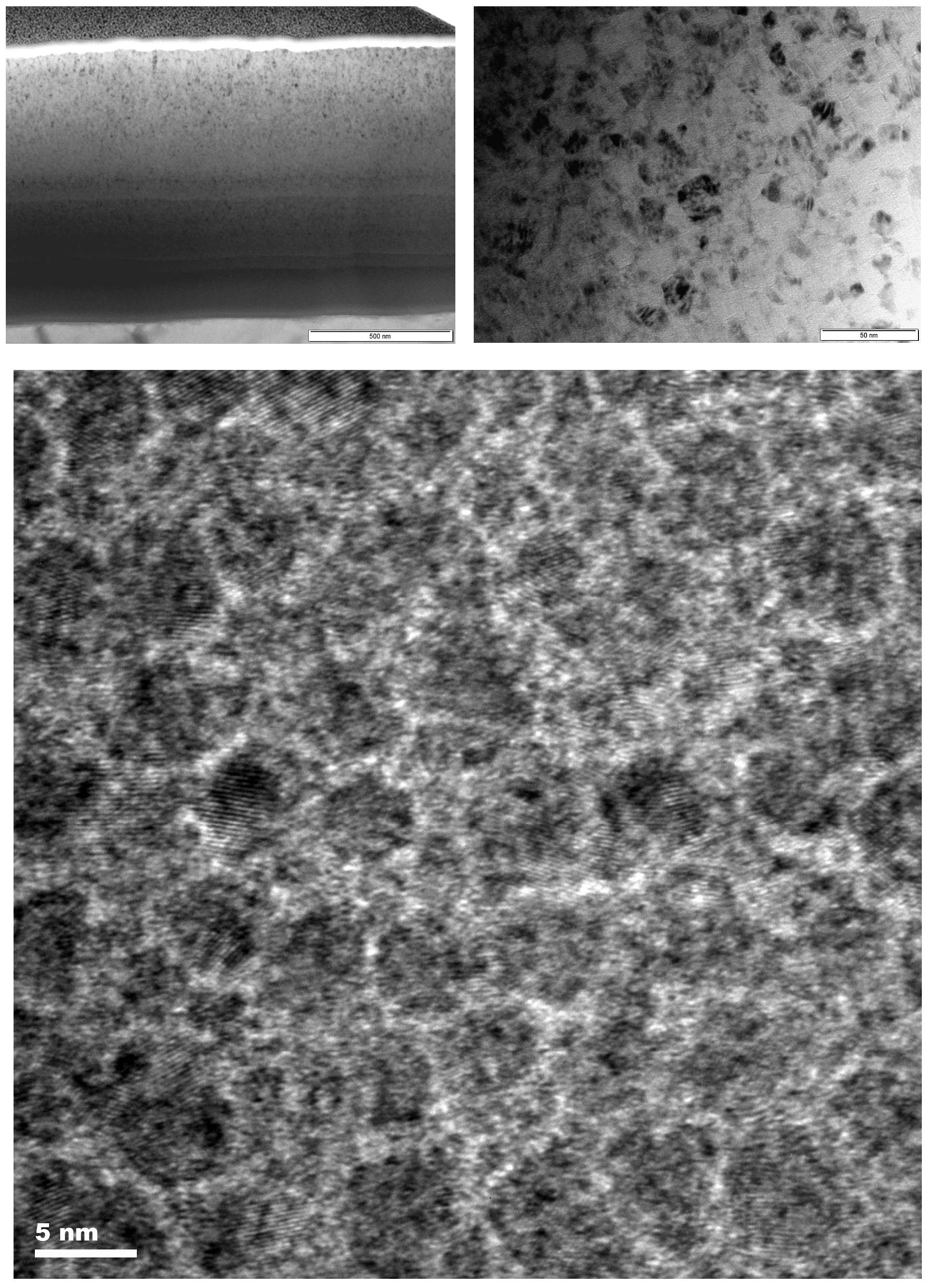
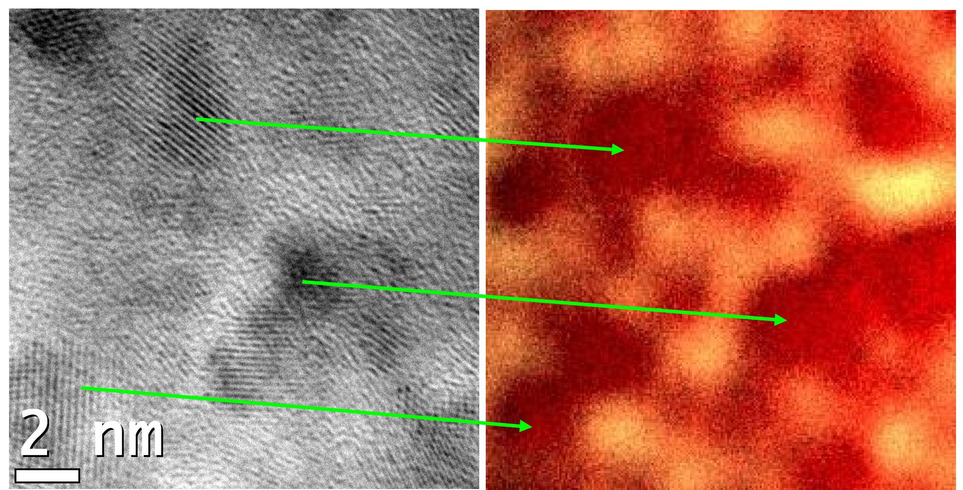
The change of sample preparation routine from cross-section to plan-view orientation enable to look along the walls of cylindrical or fibrous like grains in that type of coatings, i.e. accordingly to the scheme showed in Fig.6. The latter samples are harder to get due their highly stressed character, which causes their bending and delamination during ion milling or FIB cutting. However, changing direction of view improves observation conditions two- or threefold eliminating the superposition of crystallites. This approach is even more profitable in case of decreasing crystallite size like those present in (Cr,Si)N coatings with ~20 at.% Si (Fig. 7a,b). On some very thin areas the lattice imaging of as small crystallites as 5 to 10 nm is possible (Fig.7c). The last result has to taken as probably projection of real coating microstructure, as such extremely thin areas are subject of simultaneous ion damage, implantation and heating. Additionally, the brighter rims surrounding crystallites could represent the amorphous Si3N4 or just result from over-focusing. Therefore, the second independent confirmation, like the maps of local chemical compositions obtained using Gatan Energy Filtering system is very much welcomed (Fig.8). Having confirmed the hypothesis of segregation of CrN and Si3N4, i.e. formation of crystalline-amorphous nano-composite microstructure with two independent methods is its strong backing but final conclusions could be drawn only with their reasonably good reproducibility.
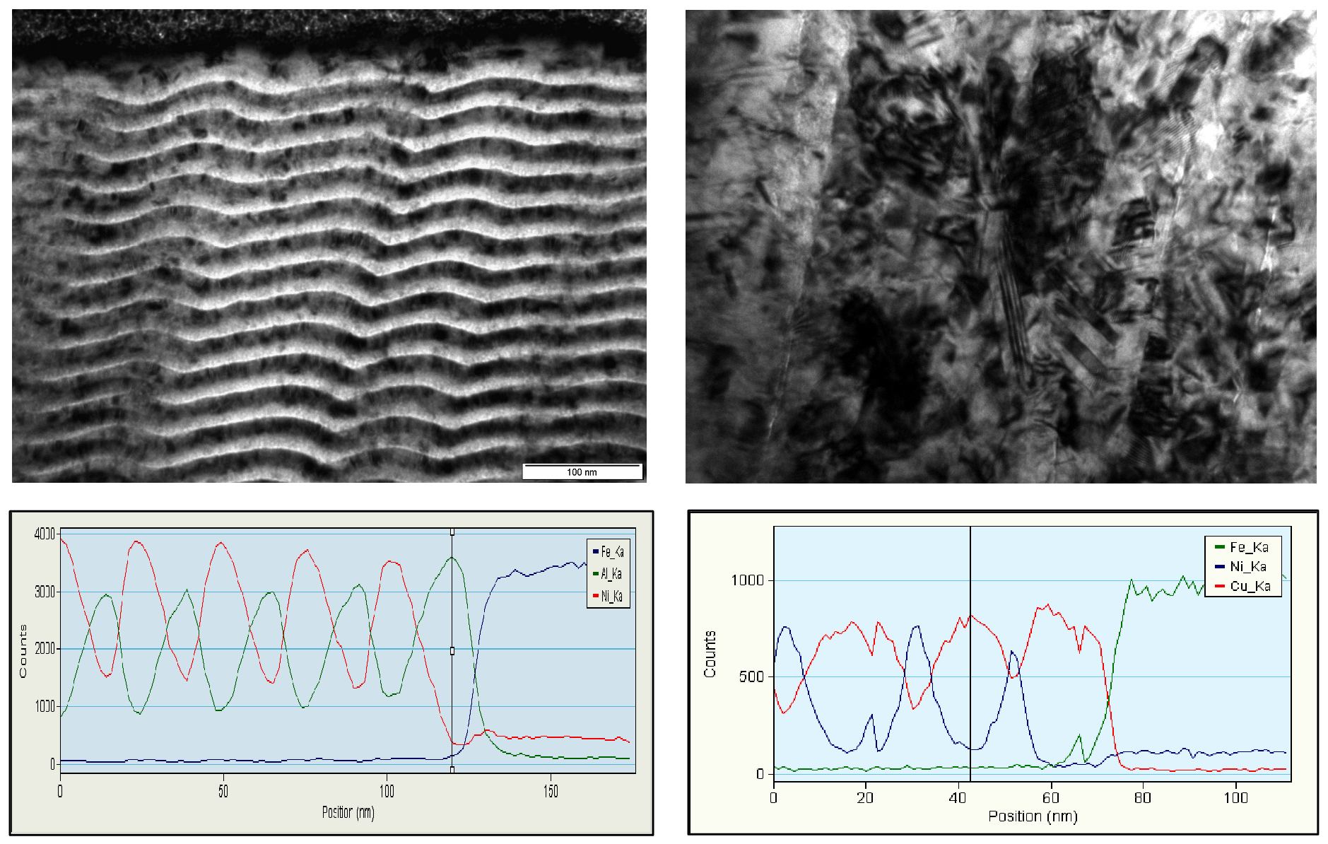
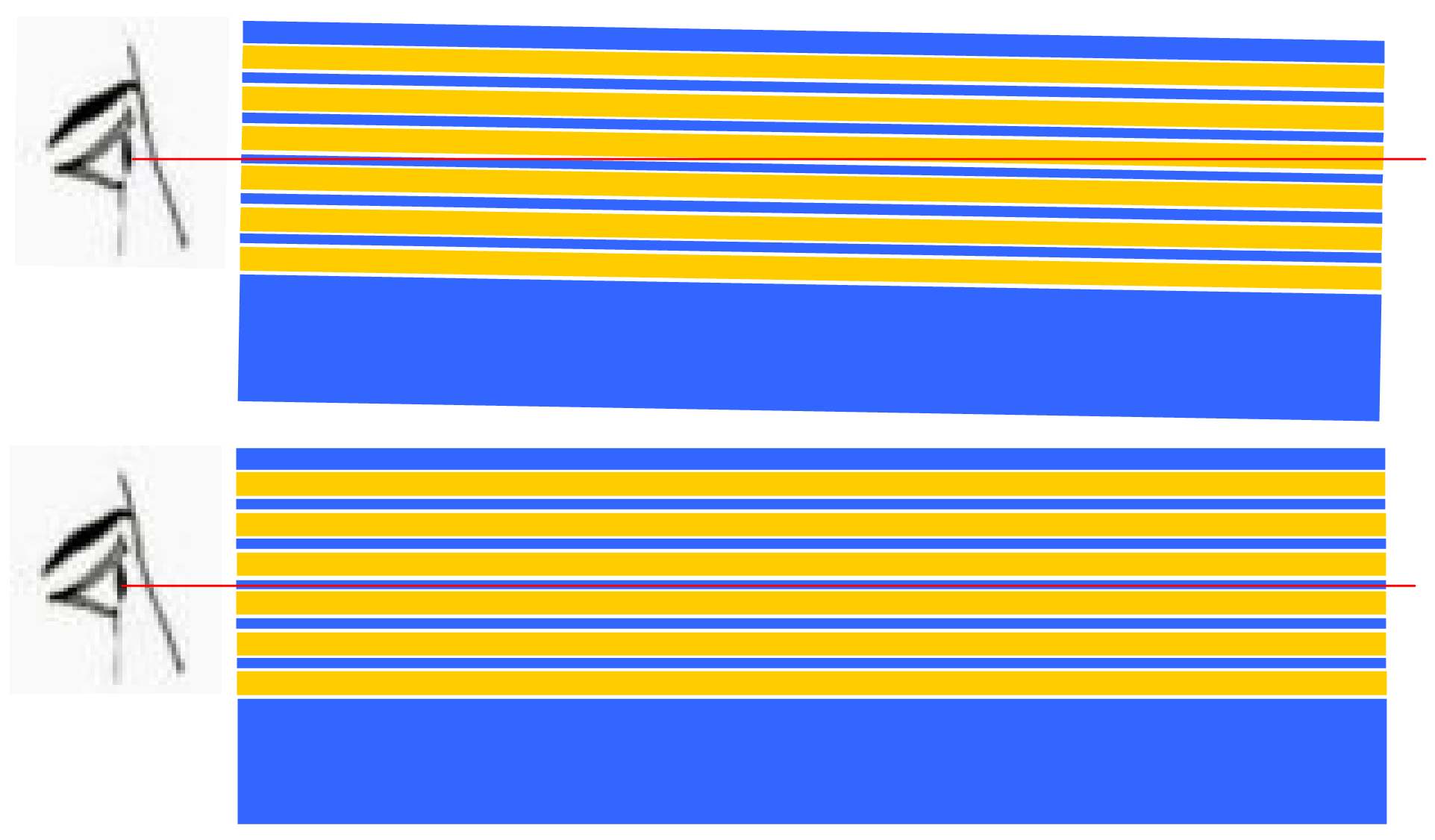
The multilayer architecture is frequently key factor to obtain property guaranteeing coatings "advanced materials" status. The general tendency is such that the finer the layers the higher the improvement. The control of multilayer coatings microstructure depends on many parameters like type of elements forming alternating layers, substrates roughness and of course multilayer period. The first part is well explained comparing multilayers of similar period ? ~ 30 nm of NiAl and CuNi coatings. The lack of mass-contrast in CuNi coatings effectively cancelled any signs of their multilayer character in BF images (Fig. 9a, b), but EDS line-scans clearly shows both real spaceings as well as some intermixing (Fig. 9c, d). The two-fold approach, i.e. imagining backed by microanalysis works relatively well down to ~10nm. However, farther down the strongest obstructions starts to turn out to be the "geometry", i.e. the FIB cut thin foil thickness rarely smaller that 100 nm (for large area specimens), beam divergence (a few nm) and the mounting of the specimen in the sample holder (a few deg relative to holder perpendicular axis). The simple trigonometry consideration indicate, that even assuming zero beam divergence the beam passage in 1nm layer will be close just with the 1/2 1 deg tilt (Fig.10). Fortunately, coatings of that type are usually deposited on single crystalline substrate what may help to fix the biggest problem, i.e.
layers - electron beam misorientation. Using Convergent Beam Electron Diffraction one may precisely, i.e. with ~0.1 deg accuracy, turn the [110]Si direction along the beam line and the deposited layers will follow. Adding some over-focusing brings multilayers forward even for quite similar layers like iron and chromium (Fig. 11).
Summary
The advanced materials present significant improvement as compared to their standard counterparts but it is usually gained through scaling down of their microstructure. The transmission electron microscopy theoretically should cope with most of the problems but real life shows that success is not so easy to get and sometimes failure looms ahead. Investigating advanced materials we need really "high level" information and the key to success is a good design of the experiments. Therefore, the more we know of the material as we start analysis the more precise information could be drawn from the performed observations and measurements. The complementary approach available while performing investigations with transmission electron microscopy frequently decides of the final success.
back


